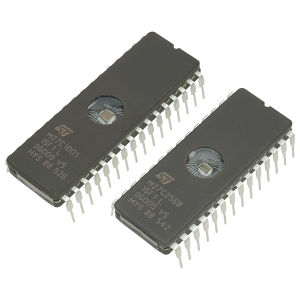
M27C256B
This device is considered obsolete.
256 Kbit (32Kb × 8) UV EPROM and OTP EPROM
Feature summary
- 5V ± 10% supply voltage in Read operation
- Access time: 45ns
- Low power consumption:
- Active Current 30mA at 5MHz
- Standby Current 100μA
- Programming voltage: 12.75V ± 0.25V
- Programming time: 100μs/Word
- Electronic signature
- Manufacturer Code: 20h
- Device Code: 8Dh
- ECOPACK® packages available
Summary description
The M27C256B is a 256 Kbit EPROM offered in the two ranges UV (ultra violet erase) and OTP (one time programmable). It is ideally suited for microprocessor systems and is organized as 32,768 by 8 bits.
The FDIP28W (window ceramic frit-seal package) has a transparent lid which allows the user to expose the chip to ultraviolet light to erase the bit pattern. A new pattern can then be written to the device by following the programming procedure.
For applications where the content is programmed only one time and erasure is not required, the M27C256B is offered in PDIP28 and PLCC32 packages.
In order to meet environmental requirements, ST offers the M27C256B in ECOPACK® packages.
ECOPACK packages are Lead-free. The category of second Level Interconnect is marked on the package and on the inner box label, in compliance with JEDEC Standard JESD97.
The maximum ratings related to soldering conditions are also marked on the inner box label.
ECOPACK is an ST trademark. ECOPACK specifications are available at: www.st.com.
Programming
When delivered (and after each erasure for UV EPROM), all bits of the M27C256B are in the "1" state. Data is introduced by selectively programming "0"s into the desired bit locations.
Although only "0"s will be programmed, both "1"s and "0"s can be present in the data word.
The only way to change a '0' to a '1' is by die exposure to ultraviolet light (UV EPROM). The M27C256B is in the programming mode when VPP input is at 12.75V, G is at VIH and E is pulsed to VIL. The data to be programmed is applied to 8 bits in parallel to the data output pins. The levels required for the address and data inputs are TTL. VCC is specified to be 6.25V ± 0.25 V.
